(Hong Kong)

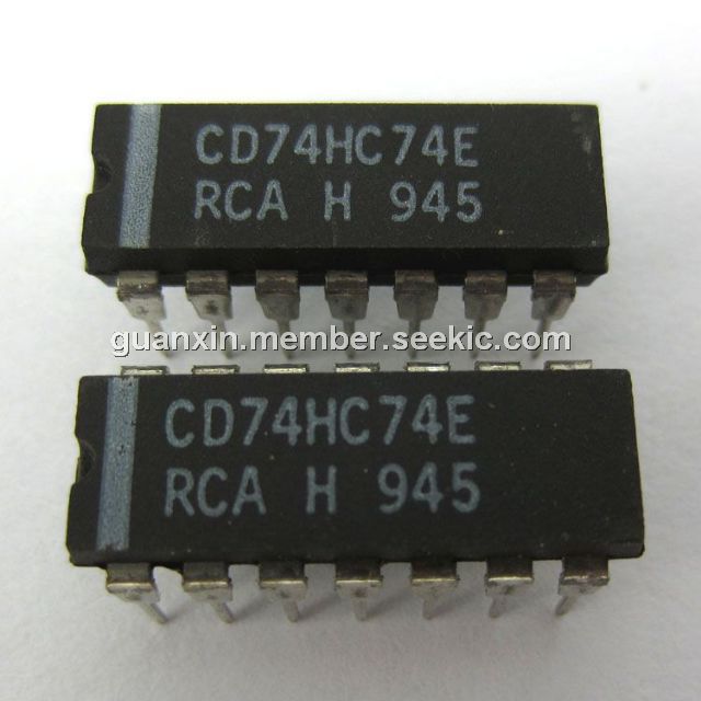
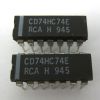
Product Summary
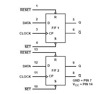
The CD74HC74E is a Dual D Flip-Flop with Set and Reset Positive-Edge Trigger. The CD74HC74E utilizes silicon gate CMOS technology to achieve operating speeds equivalent to LSTTL parts. It exhibits the low power consumption of standard CMOS integrated circuits, together with the ability to drive 10 LSTTL loads.
Parametrics
CD74HC74E absolute maximum ratings: (1)DC Supply Voltage, VCC: -0.5V to 7V; (2)DC Input Diode Current, IIK For VI<-0.5V or VI>VCC + 0.5V: ±20mA; (3)DC Drain Current, per Output, IO For -0.5V<VO<VCC + 0.5V: ±25mA; (4)DC Output Diode Current, IOK For VO<-0.5V or VO>VCC + 0.5V: ±20mA; (5)DC Output Source or Sink Current per Output Pin, IO For VO>-0.5V or VO<VCC + 0.5V: ±25mA; (6)DC VCC or Ground Current, ICC: ±50mA.
Features
CD74HC74E features: (1)Hysteresis on Clock Inputs for Improved Noise Immunity and Increased Input Rise and Fall Times; (2)Asynchronous Set and Reset; (3)Complementary Outputs; (4)Buffered Inputs; (5)Typical fMAX = 50MHz at VCC = 5V, CL = 15pF, TA = 25℃; (6)Fanout (Over Temperature Range): Standard Outputs: 10 LSTTL Loads; (7)Bus Driver Outputs: 15 LSTTL Loads; (8)Wide Operating Temperature Range: -55℃ to 125℃; (9)Balanced Propagation Delay and Transition Times; (10)Significant Power Reduction Compared to LSTTL Logic ICs; (11)HC Types: 2V to 6V Operation; (12)High Noise Immunity: NIL = 30%, NIH = 30% of VCC at VCC = 5V; (13)HCT Types: 4.5V to 5.5V Operation; (14)Direct LSTTL Input Logic Compatibility,; (15)VIL= 0.8V (Max), VIH = 2V (Min): CMOS Input Compatibility, Il≤ 1μA at VOL, VOH.
Diagrams
| Image | Part No | Mfg | Description |  |
Pricing (USD) |
Quantity | ||||||||||||
|---|---|---|---|---|---|---|---|---|---|---|---|---|---|---|---|---|---|---|
 |
 CD74HC74E |
Texas Instruments |
Flip Flops Dual |
Data Sheet |
|
|
||||||||||||
|
CD74HC74EE4 |
Texas Instruments |
Flip Flops Hi-Sp CMOS Dual Pos D-Type Flip-Flop |
Data Sheet |
|
|
||||||||||||